


Many times, unconventional PCB shapes occur because of the need to fit into oddly shaped enclosures. We will take a look at creating a panel for irregularly shaped pcbs.
1. Copy the board file and project file. Create a folder as panel and paste board file and project file into it.

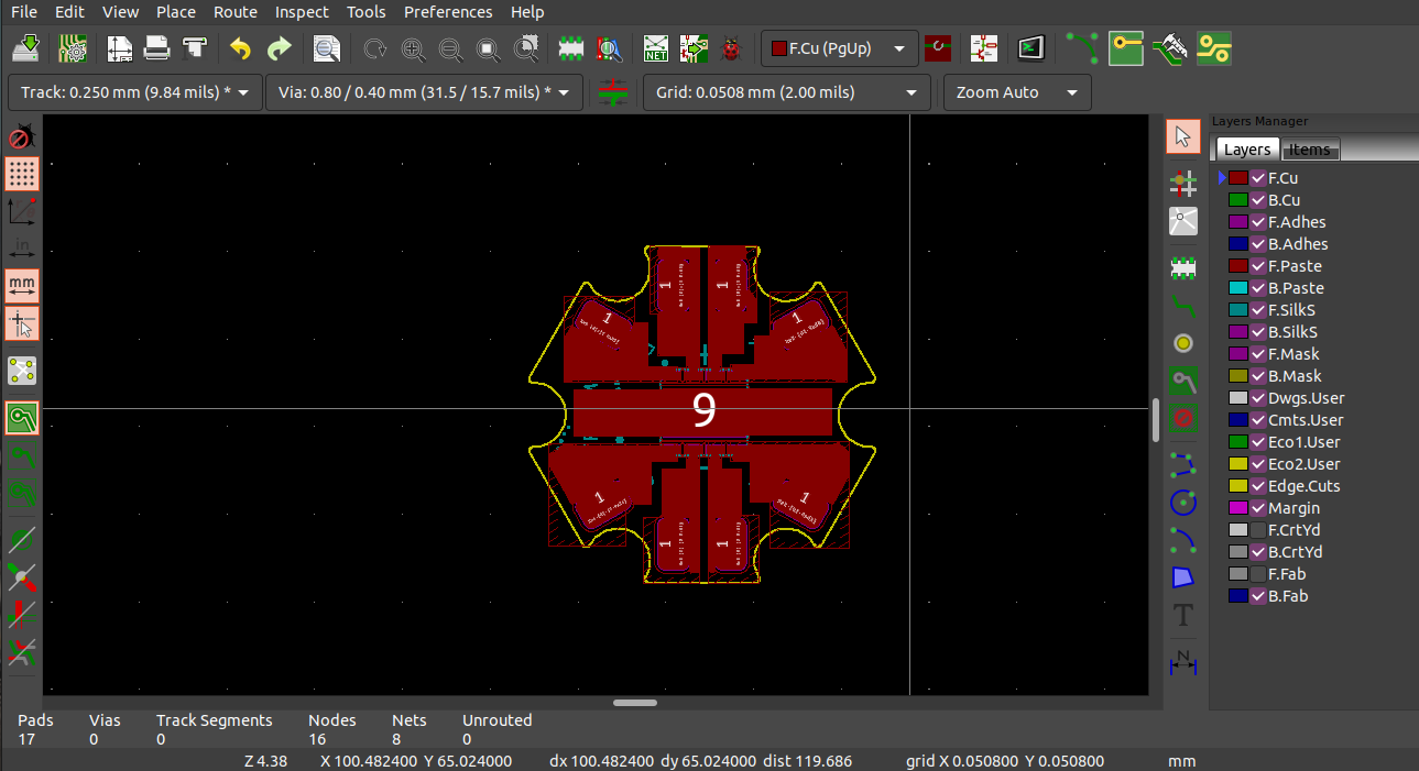
2. Open Kicad and go to the board file
3. Select the whole board file, then right click and go to create array. Set values for Horizontal count, Vertical count, Horizontal spacing, Vertical spacing as required, then click OK.

4. Click the RatsNest button and the air wires will disappear.

5. Make outlines for the panelised pcbs.


6. Check 3D viewer and make sure that outlines are correct. If outlines are correct, we will get 3D correctly otherwise make corrections. If 3D rendering is correct, then generate the Gerber file.

7. There should not be any discontinuity in the outline like as shown below.

8. If outlines are not determined correctly, 3D view will not get rendered properly.
